- 您现在的位置:买卖IC网 > Sheet目录3886 > PIC16F1827-I/ML (Microchip Technology)IC PIC MCU FLASH 4K 28-QFN
186
2570N–AVR–05/11
ATmega325/3250/645/6450
an interrupt when the transfer is complete. Note that when an external clock source is selected
the counter counts both clock edges. In this case the counter counts the number of edges, and
not the number of bits. The clock can be selected from three different sources: The USCK pin,
Timer/Counter0 Compare Match or from software.
The Two-wire clock control unit can generate an interrupt when a start condition is detected on
the Two-wire bus. It can also generate wait states by holding the clock pin low after a start con-
dition is detected, or after the counter overflows.
21.2
Functional Descriptions
21.2.1
Three-wire Mode
The USI Three-wire mode is compliant to the Serial Peripheral Interface (SPI) mode 0 and 1, but
does not have the slave select (SS) pin functionality. However, this feature can be implemented
in software if necessary. Pin names used by this mode are: DI, DO, and USCK.
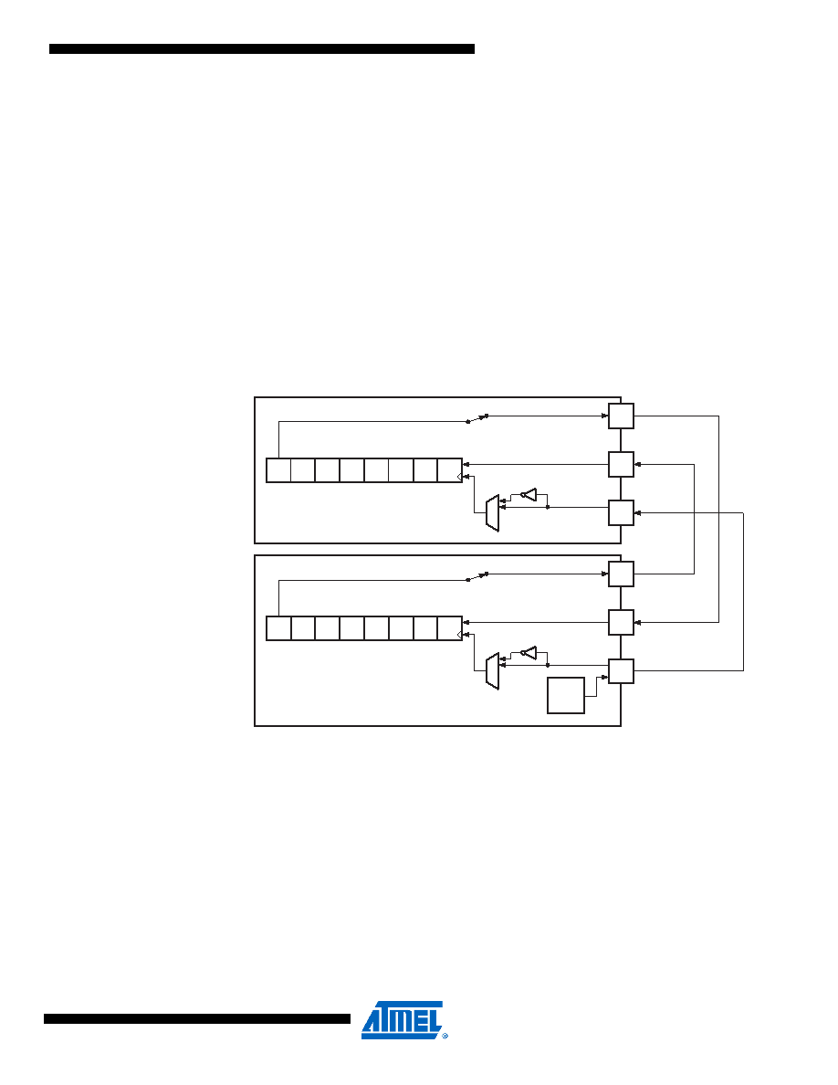
Figure 21-2. Three-wire Mode Operation, Simplified Diagram
Figure 21-2 shows two USI units operating in Three-wire mode, one as Master and one as
Slave. The two Shift Registers are interconnected in such way that after eight USCK clocks, the
data in each register are interchanged. The same clock also increments the USI’s 4-bit counter.
The Counter Overflow (interrupt) Flag, or USIOIF, can therefore be used to determine when a
transfer is completed. The clock is generated by the Master device software by toggling the
USCK pin via the PORT Register or by writing a one to the USITC bit in USICR.
SLAVE
MASTER
Bit7
Bit6
Bit5
Bit4
Bit3
Bit2
Bit1
Bit0
DO
DI
USCK
Bit7
Bit6
Bit5
Bit4
Bit3
Bit2
Bit1
Bit0
DO
DI
USCK
PORTxn
发布紧急采购,3分钟左右您将得到回复。
相关PDF资料
PIC16LCE624T-04E/SO
IC MCU CMOS 1K OTP W/EEPRM18SOIC
PIC16LF1827-I/ML
IC PIC MCU FLASH 4K 28-QFN
PIC16LCE624-04E/SS
IC MCU CMOS 1K OTP W/EEPRM20SSOP
PIC16F687-I/P
IC PIC MCU FLASH 2KX14 20DIP
PIC16LF1829-I/SO
MCU PIC 14KB FLASH 20-SOIC
PIC16LCE624-04E/SO
IC MCU CMOS 1K OTP W/EEPRM18SOIC
PIC16F1829-I/SO
MCU PIC 14K FLASH 1K RAM 20SOIC
PIC16F685-I/SS
IC PIC MCU FLASH 4KX14 20SSOP
相关代理商/技术参数
PIC16F1827-I/MQ
功能描述:8位微控制器 -MCU 7KB Flash 384 byte 32 MHz Int. Osc RoHS:否 制造商:Silicon Labs 核心:8051 处理器系列:C8051F39x 数据总线宽度:8 bit 最大时钟频率:50 MHz 程序存储器大小:16 KB 数据 RAM 大小:1 KB 片上 ADC:Yes 工作电源电压:1.8 V to 3.6 V 工作温度范围:- 40 C to + 105 C 封装 / 箱体:QFN-20 安装风格:SMD/SMT
PIC16F1827-I/MV
功能描述:8位微控制器 -MCU 7KB Flash 384 RAM RoHS:否 制造商:Silicon Labs 核心:8051 处理器系列:C8051F39x 数据总线宽度:8 bit 最大时钟频率:50 MHz 程序存储器大小:16 KB 数据 RAM 大小:1 KB 片上 ADC:Yes 工作电源电压:1.8 V to 3.6 V 工作温度范围:- 40 C to + 105 C 封装 / 箱体:QFN-20 安装风格:SMD/SMT
PIC16F1827-I/P
功能描述:8位微控制器 -MCU 7KB Flash 384 byte 32 MHz Int. Osc RoHS:否 制造商:Silicon Labs 核心:8051 处理器系列:C8051F39x 数据总线宽度:8 bit 最大时钟频率:50 MHz 程序存储器大小:16 KB 数据 RAM 大小:1 KB 片上 ADC:Yes 工作电源电压:1.8 V to 3.6 V 工作温度范围:- 40 C to + 105 C 封装 / 箱体:QFN-20 安装风格:SMD/SMT
PIC16F1827-I/SO
功能描述:8位微控制器 -MCU 7KB Flash 384 byte 32 MHz Int. Osc RoHS:否 制造商:Silicon Labs 核心:8051 处理器系列:C8051F39x 数据总线宽度:8 bit 最大时钟频率:50 MHz 程序存储器大小:16 KB 数据 RAM 大小:1 KB 片上 ADC:Yes 工作电源电压:1.8 V to 3.6 V 工作温度范围:- 40 C to + 105 C 封装 / 箱体:QFN-20 安装风格:SMD/SMT
PIC16F1827-I/SS
功能描述:8位微控制器 -MCU 7KB Flash 384 byte 32 MHz Int. Osc RoHS:否 制造商:Silicon Labs 核心:8051 处理器系列:C8051F39x 数据总线宽度:8 bit 最大时钟频率:50 MHz 程序存储器大小:16 KB 数据 RAM 大小:1 KB 片上 ADC:Yes 工作电源电压:1.8 V to 3.6 V 工作温度范围:- 40 C to + 105 C 封装 / 箱体:QFN-20 安装风格:SMD/SMT
PIC16F1827T-I/ML
功能描述:8位微控制器 -MCU 7KB Flash 384 byte 32 MHz Int. Osc RoHS:否 制造商:Silicon Labs 核心:8051 处理器系列:C8051F39x 数据总线宽度:8 bit 最大时钟频率:50 MHz 程序存储器大小:16 KB 数据 RAM 大小:1 KB 片上 ADC:Yes 工作电源电压:1.8 V to 3.6 V 工作温度范围:- 40 C to + 105 C 封装 / 箱体:QFN-20 安装风格:SMD/SMT
PIC16F1827T-I/MQ
功能描述:8位微控制器 -MCU 7KB Flash 384 byte 32 MHz Int. Osc RoHS:否 制造商:Silicon Labs 核心:8051 处理器系列:C8051F39x 数据总线宽度:8 bit 最大时钟频率:50 MHz 程序存储器大小:16 KB 数据 RAM 大小:1 KB 片上 ADC:Yes 工作电源电压:1.8 V to 3.6 V 工作温度范围:- 40 C to + 105 C 封装 / 箱体:QFN-20 安装风格:SMD/SMT
PIC16F1827T-I/MV
功能描述:8位微控制器 -MCU 7KB Flash 384 RAM RoHS:否 制造商:Silicon Labs 核心:8051 处理器系列:C8051F39x 数据总线宽度:8 bit 最大时钟频率:50 MHz 程序存储器大小:16 KB 数据 RAM 大小:1 KB 片上 ADC:Yes 工作电源电压:1.8 V to 3.6 V 工作温度范围:- 40 C to + 105 C 封装 / 箱体:QFN-20 安装风格:SMD/SMT